JEE Main 2019 — Semiconductors Question with Solution
JEE Main 2019 (12 Apr Shift 1)
Question
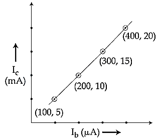
The transfer characteristic curve of a transistor, having input and output resistance and respectively, is shown in the figure. The voltage and power gain, are respectively:
Choose an option
Show full solutionCorrect option: A
Correct answer
A
Step-by-step explanation
Current gain
Voltage gain
Power gain
Voltage gain
Power gain
Practice this on the real CBT interface
Solve this JEE Main question (and the rest of the Semiconductors chapter) on PrepSharp's TCS iON-style CBT player — with timer, bookmarks and session analytics.
Solve interactively →About this question
This is a previous-year question from JEE Main 2019, covering the Semiconductors chapter of Physics. PrepSharp catalogues every PYQ from JEE Main with a verified answer key and step-by-step solution prepared by IIT alumni — so you can search by chapter, topic or year and revise efficiently.